(China (Mainland))

Product Summary
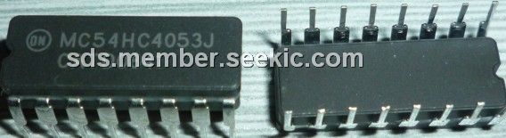
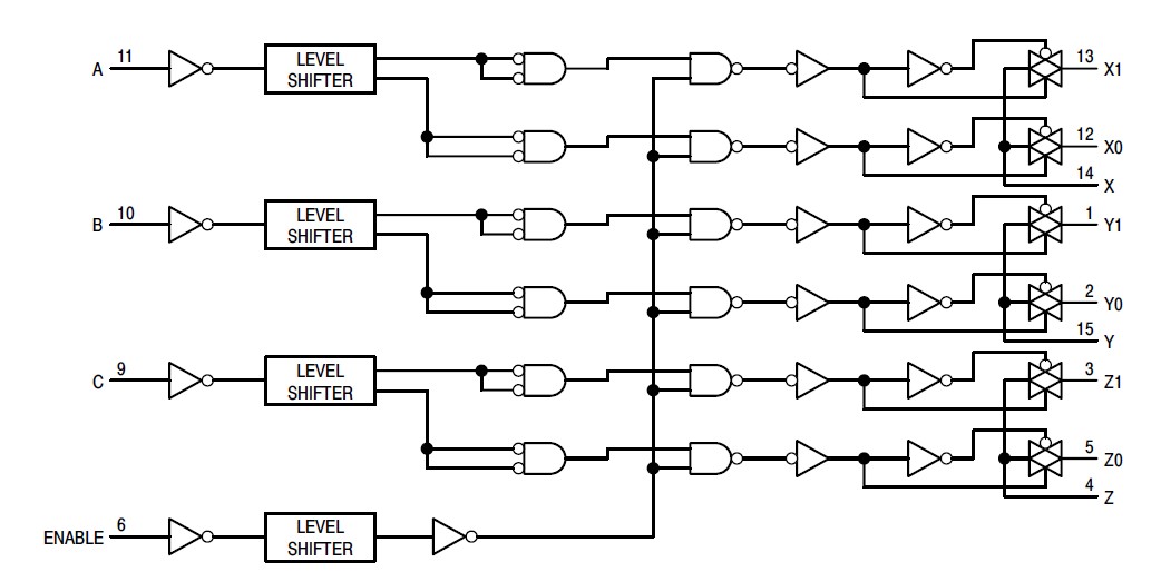
The MC54HC4053J is an analog multiplexer/ demultiplexer. The MC54HC4053J controls analog voltages that may vary across the complete power supply range (from VCC to VEE). The MC54HC4053J is identical in pinout to the metal–gate MC14051B, MC14052B and MC14053B. The Channel–Select inputs of the MC54HC4053J determine which one of the Analog Inputs/Outputs is to be connected, by means of an analog switch, to the Common Output/Input. When the Enable pin is HIGH, all analog switches are turned off. The Channel–Select and Enable inputs are compatible with standard CMOS outputs; with pullup resistors they are compatible with LSTTL outputs.
Parametrics
MC54HC4053J absolute maximum ratings: (1)VCC Positive DC Supply Voltage (Referenced to GND)(Referenced to VEE): 2.0 to 12.0V; (2)VEE Negative DC Supply Voltage, Output (Referenced to GND): – 6.0 to GND V; (3)VIS Analog Input Voltage VEE: VCCV; (4)Vin Digital Input Voltage (Referenced to GND)GND: VCC V; (5)VIO Static or Dynamic Voltage Across Switch: 1.2 V; (6)TA Operating Temperature Range, All Package Types: – 55 to + 125℃; (7)tr, tf Input Rise/Fall Time VCC = 2.0 V (Channel Select or Enable Inputs)VCC = 4.5 V VCC = 6.0 V: 1000 ns.
Features
MC54HC4053J features: (1)Fast Switching and Propagation Speeds; (2)Low Crosstalk Between Switches; (3)Diode Protection on All Inputs/Outputs; (4)Analog Power Supply Range (VCC – VEE)= 2.0 to 12.0 V; (5)Digital (Control)Power Supply Range (VCC – GND)= 2.0 to 6.0 V; (6)Improved Linearity and Lower ON Resistance Than Metal–Gate Counterparts; (7)Low Noise; (8)In Compliance With the Requirements of JEDEC Standard No. 7A.
Diagrams
 |
 MC54 |
Other |
|
Data Sheet |
Negotiable |
|
||||
|
MC54F169 |
Other |
|
Data Sheet |
Negotiable |
|
||||
|
MC54F20 |
Other |
|
Data Sheet |
Negotiable |
|
||||
|
MC54F21 |
Other |
|
Data Sheet |
Negotiable |
|
||||
|
MC54F240 |
Other |
|
Data Sheet |
Negotiable |
|
||||
|
MC54F251 |
Other |
|
Data Sheet |
Negotiable |
|
||||